Huawei’s Nerves of Steel: Chinese Tech Giant Overcomes US Ban with Innovative EUV Lithography Patent for 5G

Huawei is again showing nerves of steel; despite the constant bans and restrictions from the US government, the Chinese tech giant has continued to brave the wave and is proving more resilient every day.
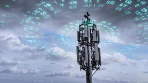
The bans Huawei has received in the last three years since the dawn of COVID 19 would cripple any company. However, as the data shows, Huawei might be struggling but not to the extent any of us thought they would. Aside from the play store ban, Huawei faces a ban against installing 5g on their devices. However, the company may have found a workaround to this scenario.
Huawei may have found a solution to its current problem by using EUV lithography, a microfabrication technology that creates delicate patterns on a substrate using EUV light. Researchers can use these patterns to build complex microelectronic structures, such as microchips in the manufacturing process of semiconductor devices.”
The Patent
According to the report, the patent application needs a go-ahead from China’s National Intellectual Property Administration and is awaiting approval.
It also needs to be determined whether Huawei can manufacture a complete EUV machine, which is a complex machine that contains over 100,000 components. However, the patent application details suggest that Huawei may have identified a solution to an issue related to EUV technology, which involves using a more uniform light source.
ASML, in the Netherlands, is currently the only manufacturer of EUV equipment in the world, and they filed a similar patent in 2016. However, the patent filed by ASML reportedly differs from Huawei’s patent in how the technology utilizes light in the EUV process.
The Hack
According to the report, Huawei is working on using optoelectronic wafers and other innovative approaches to bypass lithography. Optoelectronic wafers can create optoelectronic devices, such as light-emitting diodes (LEDs) and photovoltaic cells.
These wafers are unique because they can produce and detect light, making them essential for many applications, including lighting, display technologies, and renewable energy. Optoelectronic wafers typically come from various materials, including silicon and indium phosphide.
Manufacturers use them to produce various optoelectronic devices, including lasers, sensors, and displays. Huawei and other developers can use these materials in various applications, including telecommunications, lighting, and solar power generation. According to the report, Huawei is exploring optoelectronic wafers to create microelectronic structures without lithography.
Developing technologies and approaches that bypass lithography is essential for the future of Huawei and China as a whole, as it could produce more advanced and efficient semiconductor devices. Companies commonly conduct research and development in this area to stay ahead of the competition and drive innovation in the industry, and Huawei is doing just that.
If the patent is approved, Huawei will help Chinese chip makers produce advanced chips for use in smartphones. This step would be significant because China is actively seeking to become more self-sufficient in producing semiconductors, which are essential components of many electronic devices, including smartphones.
By developing their EUV technology, Huawei and other Chinese companies could produce more advanced and efficient chips for their smartphones and other electronic devices.
The patent application is in the hands of the Chinese government. However, Huawei will likely know the outcome in 2023. It is common for obtaining a patent to take several months or even years, as it involves a thorough review of the technology and its potential impact.